

Quick Search:


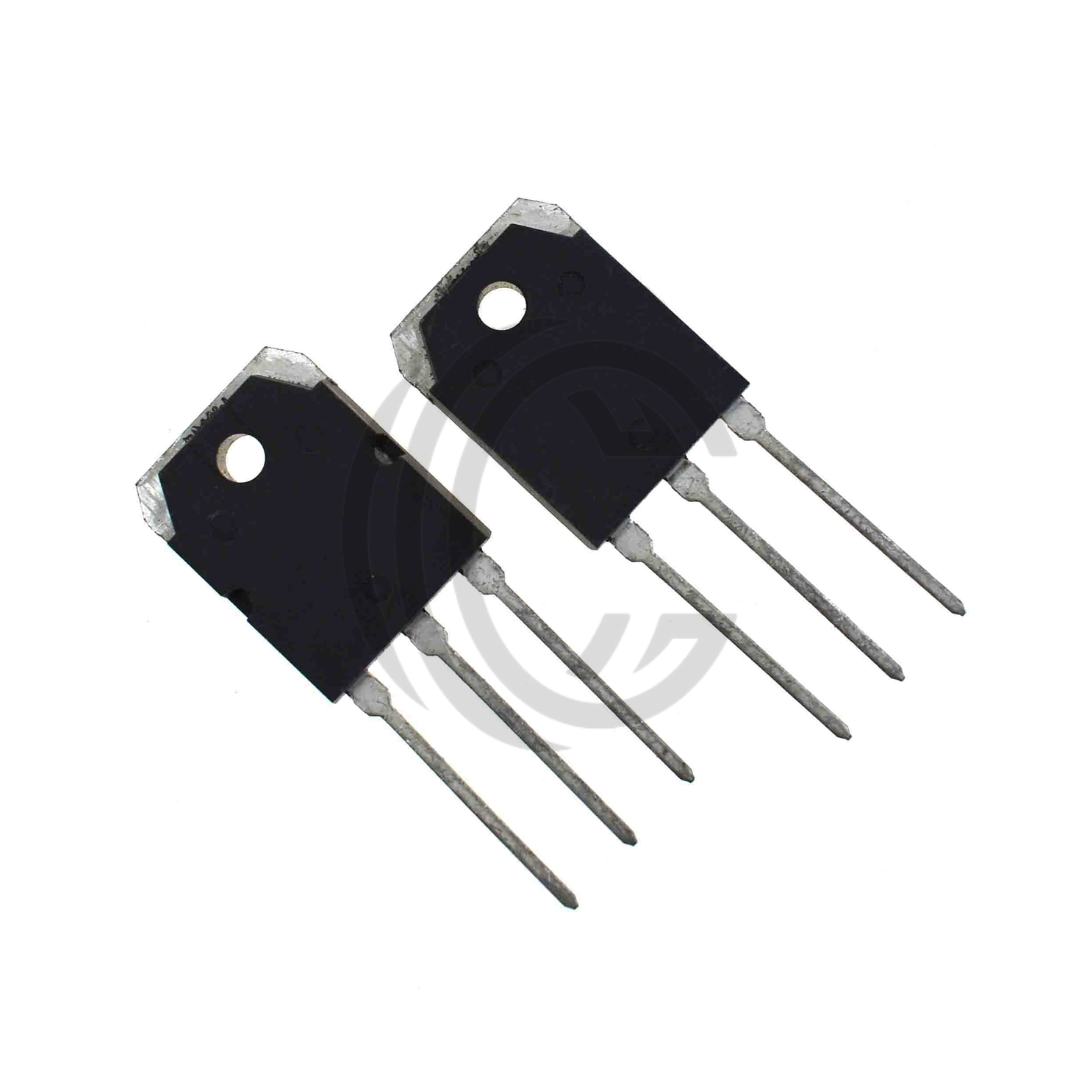
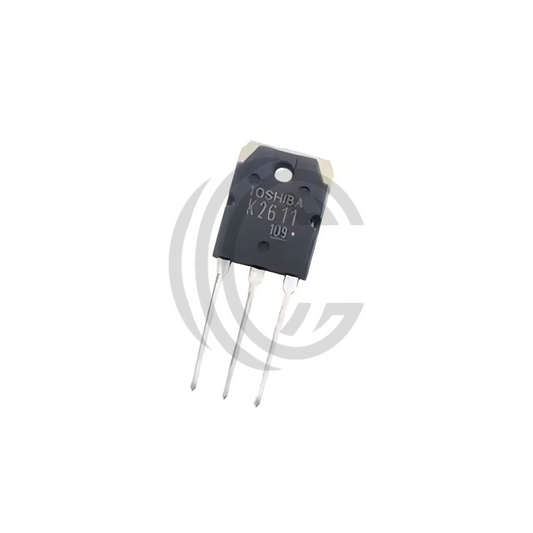
K2611 900 V 9 A N‑Channel Power MOSFET – TO‑3PN Package
The K2611 (also known as 2SK2611) is a high-voltage N‑Channel MOSFET rated for 900 V drain‑source breakdown and 9 A continuous drain current at 25 °C. Designed with planar DMOS (π‑MOS III) technology, it delivers low on-state resistance (approximately 1.1 Ω at VGS = 10 V) and exhibits fast switching capabilities with gate charge around 58–72 nC depending on variant.
It handles 150 W power dissipation (Tc = 25 °C) and supports 27 A pulse current during avalanche conditions. The device includes robust protection features such as ±30 V maximum gate voltage and a junction temperature rating up to 150 °C.
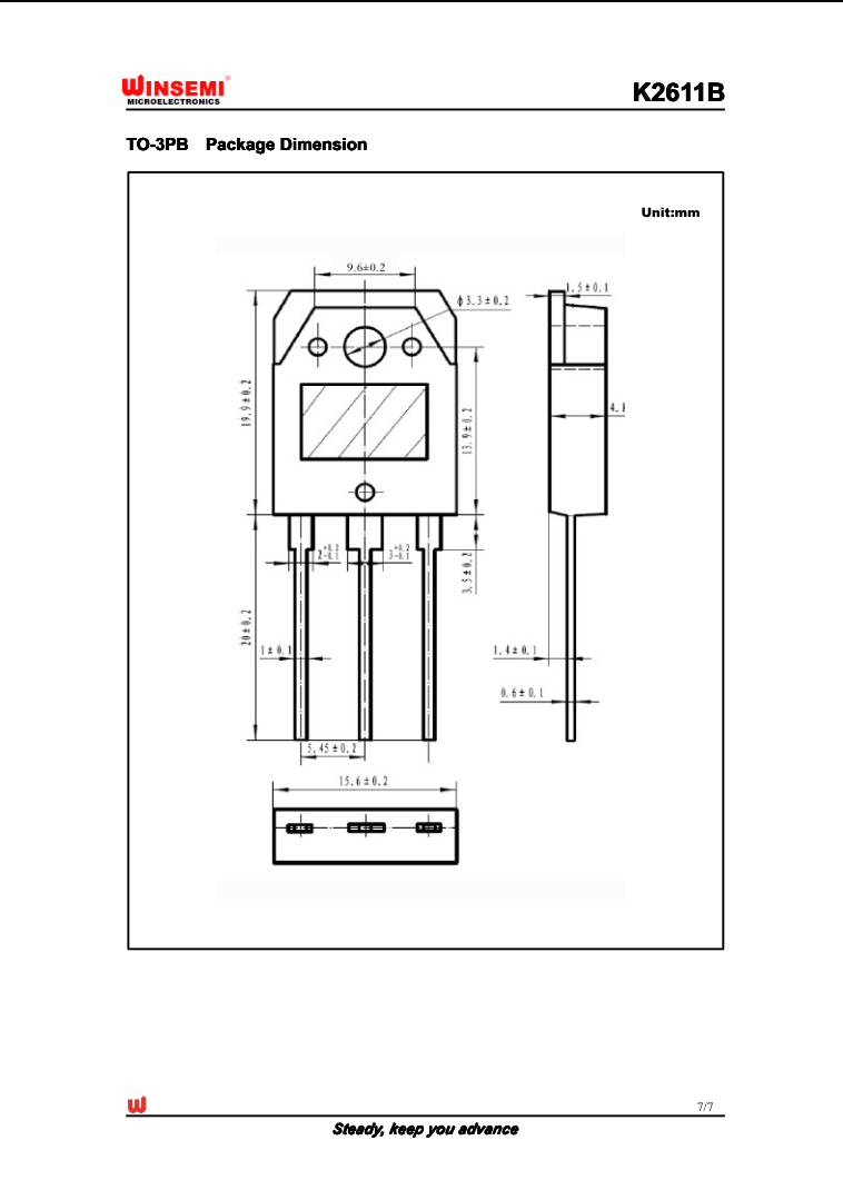
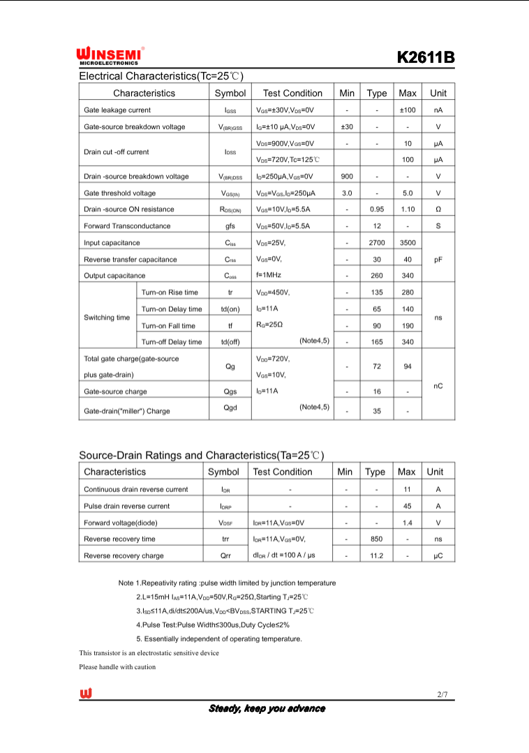
Maximum Drain-Source Voltage (VDS): 900V Continuous Drain Current (ID): 9 A @ TC = 25 °C Single-Pulse Drain Current (IDM): 27 A Maximum Power Dissipation (PD): 150 W @ TC = 25 °C RDS(on) – Drain-Source On-Resistance: ~1.1 Ω @ VGS = 10V Gate Charge (Qg): 58–72 nC (typ.) Gate-Source Voltage (VGS max): ±30 V Maximum Junction Temperature (Tj max): 150 °C Thermal Resistance (Rθj‑c): ~0.833 °C/W, Rθj‑a: ~50 °C/W Package: TO‑3PN metal can with enhanced thermal dissipation
Low RDS(on) (~1.1 Ω) for reduced conduction loss. Moderate gate charge (~58–72 nC) supports efficient switching. High-voltage rating (900 V) allows use in high-voltage switching circuits. Avalanche-tested up to 27 A pulse current for rugged performance. TO‑3PN package ensures excellent thermal handling under heavy load. Stable operation up to 150 ° C junction temperature. Gate-source tolerance up to ± 30 V enables compatibility with standard driver circuits.
We deliver all across Pakistan through trusted courier partners, including TCS and Leopards. Our nationwide shipping ensures that your order reaches you within 2 to 3 working days. Delivery charges are calculated based on the total parcel weight — for example, 1kg, 2kg, or 3kg packages may vary in cost accordingly.